Memory controller work continues….workaround 4MB SRAM add-on

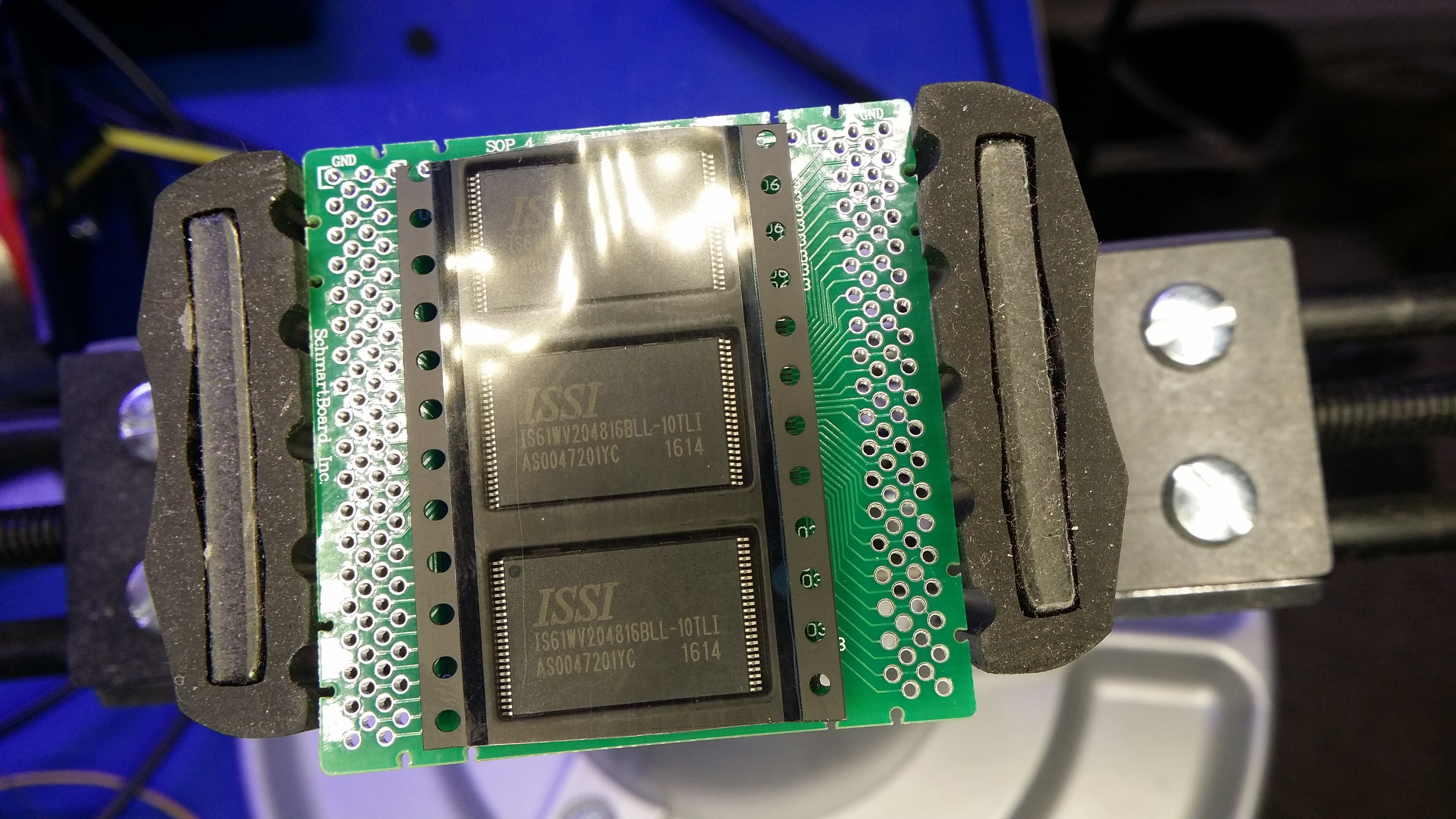
SO here’s a couple hundred dollars of SRAM parts ordered to add on to the FPGA. It goes like this: the memory controller isn’t fully integrated yet into the J68 soft-core, so I’ve decided to whack on 4 megabytes of 10-12ns SRAM. SRAM is expensive! About $24 for good quality ISSI ram.
What you see in the center of the image above are three (80) pin card edge MEC6-140 connectors that are designed to mate with the FPGA board. I needed something to mount the SRAM chip (48-pin TSOP I) on and something to mount these 80-pin connectors on. It turns out my closest match are these Schmartboard PCBs, which I’ve wanted to check out for the longest time.
It turns out that I really don’t care for these Schmartboards, partially because I don’t have the right 0.4mm tip required for the pitches, but there’s other reasons. These likely deserve their own review which I will do in a separate post.
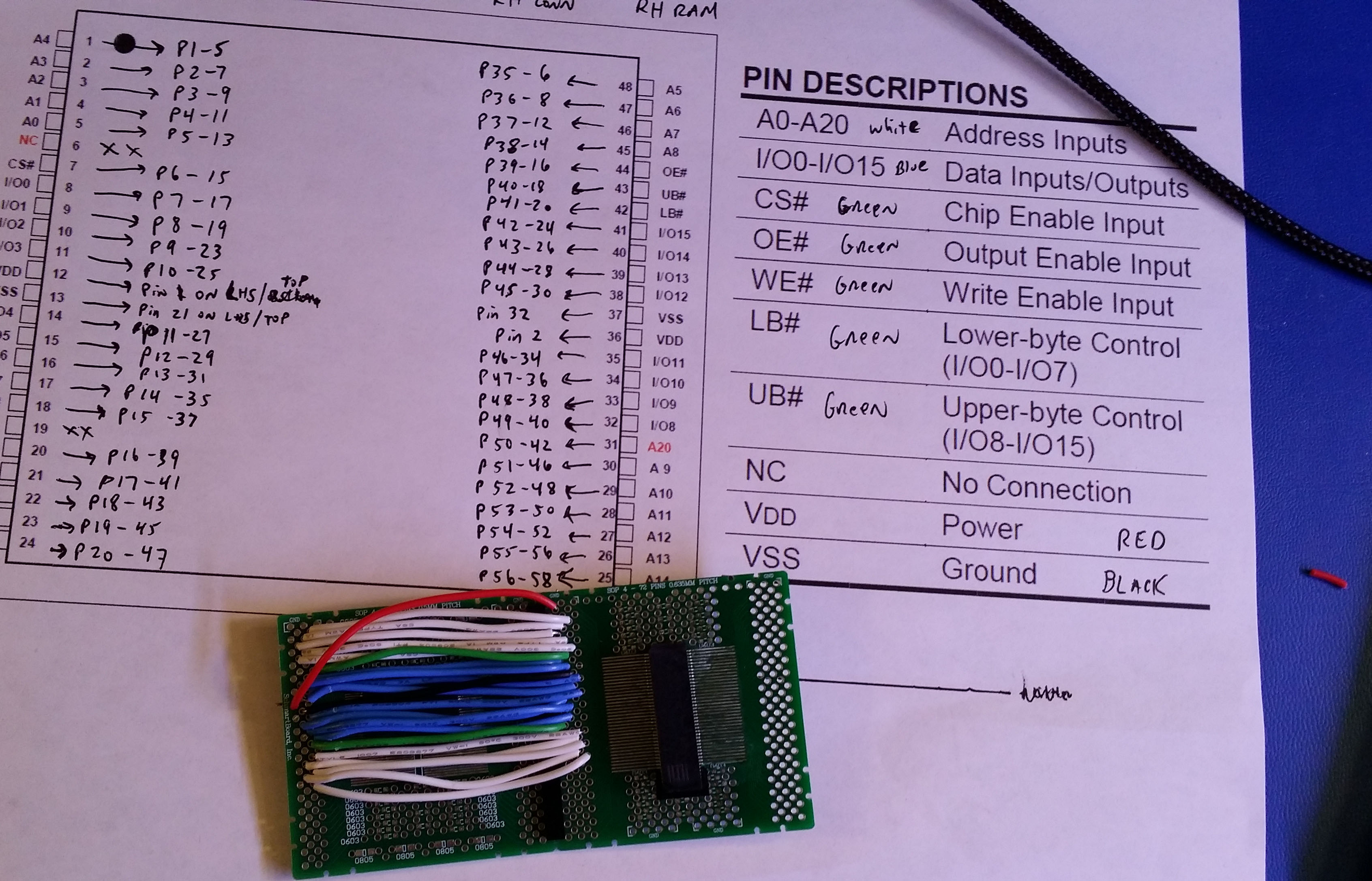
It turns out that when you are creating memory boards, you’ve got to deal with a lot of pins. How many? 16 data bits wide, 21 bits of address, plus 5 control pins, oh yeah (2) power and (2) ground as well. So that’s a solid 46 pins you’re using. The 80-pin connector has about (60) usable data pins, so at least the FPGA can support this application.
I do love the fact that the memory I’m using are 10-12ns chips. Really fast access times. Here’s a link to the digi-key part.
Here’s what $75 in memory chips looks like:
Of course you’ve got to create a pinout and hope you get everything right.
Below you’ll see a half-finished board with the 80-pin connector on the right, and the SRAM soldered to the board underneath the wires.
I’ve just recently completed the entire board, more photos to come on this.
While a couple initial writes and reads functioned, some reads or writes are failing. I need to write a small state machine that loops through all addresses, and then reads them back to check for errors.