Doing the A3660 CPU board, the first open “Seminative” 060 solution. and why.
This is the story how to reverseengineer a 040 board, and take it to the next step.
This board is shown for the first time at Amiga32 in Neuss/Germany
TL;DR: files at bottom of this post!
The Commodore A3640 is a well known CPU board for the Commodore Amiga.
It is also know as the 040 board that is ordered as the WORST CPU board ever…
AND it is true..
BUT! this board is the only we have with all data on all chips.. all GAL data is released by Dave Haynie some time ago.
Anyway. the story is as those boards suffer of leakage of the capacitors,, especially as THREE of them are from factory mounted the wrong way.. they LEAK and destroy the PCBs. they simply die.
aprox 2 years ago.. I was thinking of a good way of reparing those boards. and apprentlty one of the biggest issues is the leakage killing the PCBs. I was thinking of a way to check this.
I found the photos of bare PCBs on the internet. I asked people of making a black/white version of this so I could mix the traces so you simply could follow the traces..
And a firend of mine (Klementino Horvat in Croatia) told me he could try to make them b/w.. and well he did:
Mixed together it looked like:
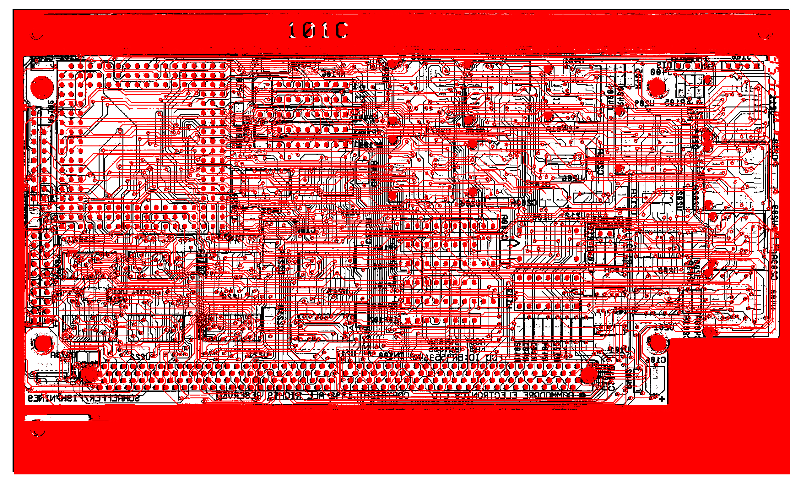
this was the first embryo for my next project:
To simply make a rerace of the A3640 board.
so I did
Render looked like:
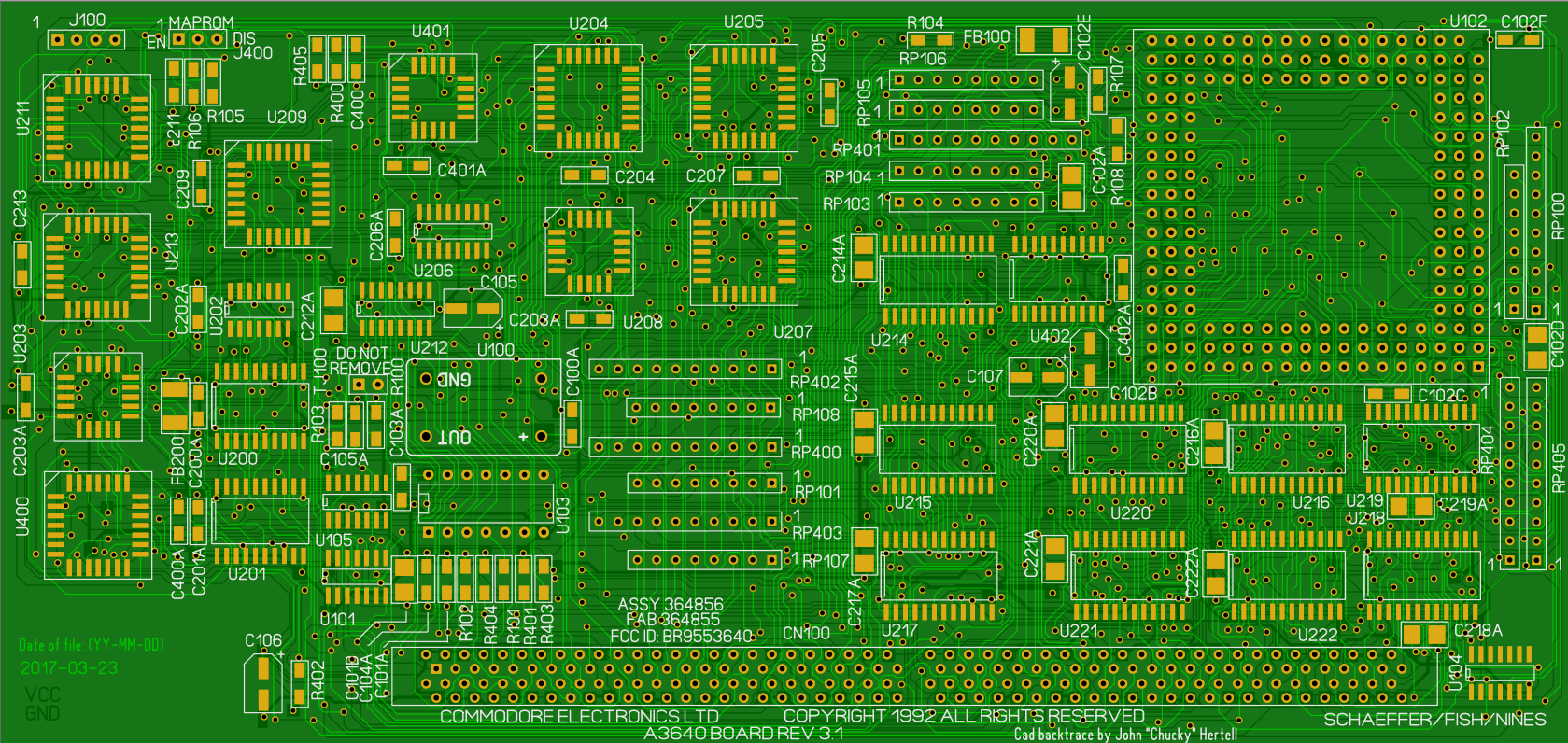
and real board:
This was my first step in producing new boards. First the 3.3 show rendered here. and then the 3.3.2 where I removed the unnecessary jumpers (J100 and the Do Not Remove jumper) also made some changes in GND and VCC planes.
and this is where I planned to stop. People asked me about implementing the 040->060 adapter but the software I am using is a pain to do changes in the PCB so.. nah..
Until I was thinking. well. hey. why not, it would be neat that I do not have to solder those damn adapters as I think they are a pain to solder. (with risking doing it wrong sending 5V to the 060 cpu etc etc)
So, I started to think.. where to put the extra 74F257 and resistors and caps? well.. first clean up traces inside the 040, making room there. putting the pullup resistors on the topside under the cpu, and putting the 74F257 on the bottomside.. took some painful hours (days) of rerouting traces:
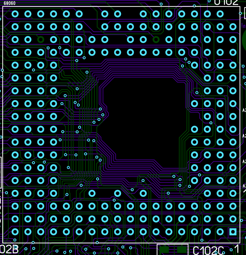
and indeed, I managed to clean up the area enough to fit the 74f257 needed for the adapter. and as I would need some resistors there, the 1206 size would not fit, so I simply changed ALL SMD components from 1206 to 0805. and as 0805 is cheaper anyway. winwin.
So now I just needed a place to put the voltregulator. and this was an issue. as I want to as close to the 060 as possible.
So.. I figured out, IF I remove the resistorpacks close to the cpu and put them on the backside, I would get space for a voltregulator.. so I did.
But after doing those. I just could not the rest of the resistorpacks be there as it looks odd with resistors on some locations and resistorpacks on some. so. I changed them all. Why did I not use SMD resistorpacks? well this is just lazyness as a reason as that would mean even MORE re-routing. so I skipped that.
So now, I had space for voltregulator and removed all holethrough resistorpacks.. time to do the 3.3V voltageplane.
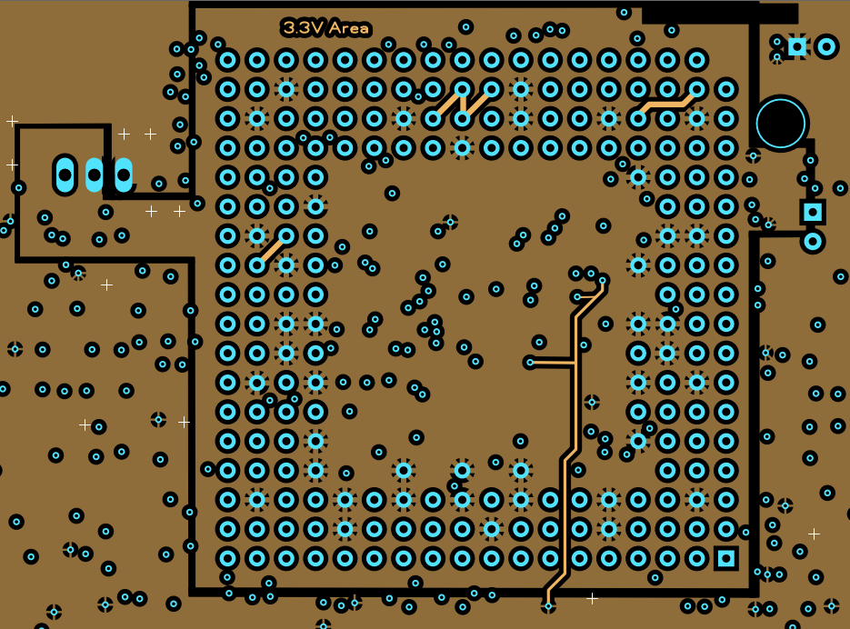
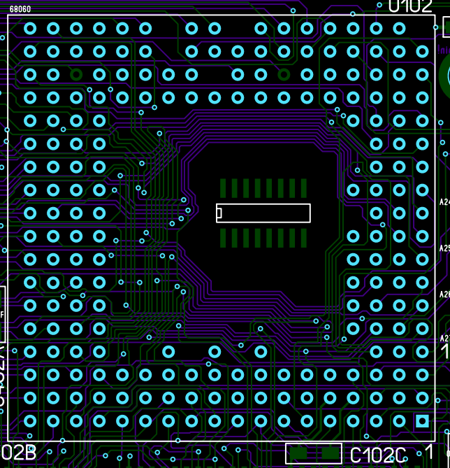
And this is how it looks like. if you wonder why there is some traces between some pins on the CPU. the explanation is in the GND plane:
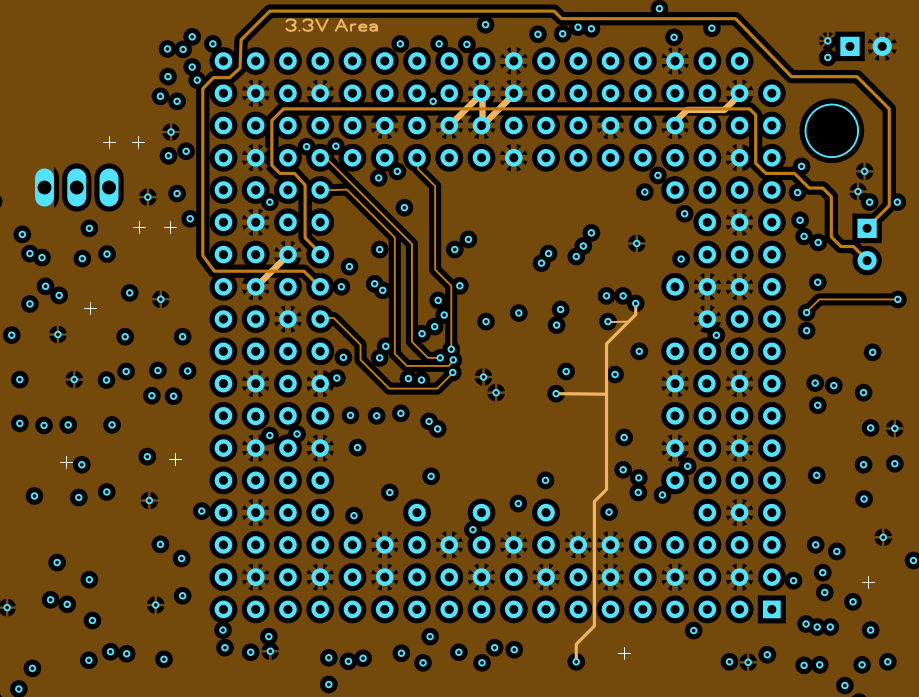
The reason is, I ran out of possabilities to do traces on upper and lower layers so I had to do some internal ones. especially to introduce the THERM0 and THERM1 pins (more about those later)
this made the GND plane there somewhat tight. that is why I added extra GND connections in the 3.3V side.
you can also see that I draw a small tiny trace from the 5V area to the 74F257 chip inside the 3.3V area, as it needs 5V to operate.
if you look at the first pictures of my retrace of the cpu socket, you can see that I originally planned to have 68060 ONLY. after talking to marmes and he gave me a simple hint of how to disable the 040-060 socket, I put back holes so you can have a 040 ASWELL. (as my original plan was.. A3660 will be 060 only)
Anyway. after a while. I got it all in there. and as there was some free space on the side of the board I added the pins THERM0 and THERM1 frm the cpu, it is internal pins from the 060 cpu that you can use to check die-temperature. there is no more connection or so except to those jumperpins. But it is now easly reachable for you to do some magic with an arduino or so to do temp-regulating or anything.
I also added a +5V powerconnector for fans. Strangly enough the CPU slot does not contain any 12V pin so no “normal” 12V fan can be used.
And there is a 040/060 “jumper” (via a 1Ohm resistor) that disables the 040-060 adapter. so if you will use a 040 on this board set that jumper to 040 mode. AND skip the voltregulator, and put a jumperwire between the IN and OUT pins of the regulator. this will make the 3.3V area having 5V instead. (do NOT connect a 060 cpu in this case or you WILL fry it)
but except this, this board is technically just a 3640 board with internal 040-060 adapter. So this have a drawback. IF you have a full 060 cpu (with FPU) your machine WILL end at a endless guru. So you still will need a custom kickstart that disables the FPU at poweron. (that setpatch later enables.) and this is the reason I call this a “Seminative” 060 card. YES you can have the 060 CPU with no adapter. BUT as this still lack a ROM that disables the FPU at poweron as ordinary native 060 cards does and is dependent of a custom rom. this will so far only SEMInative 060.
BUT as adapter is not required, this WILL also fit in an A3000.
ANYWAY!? the result you may ask?
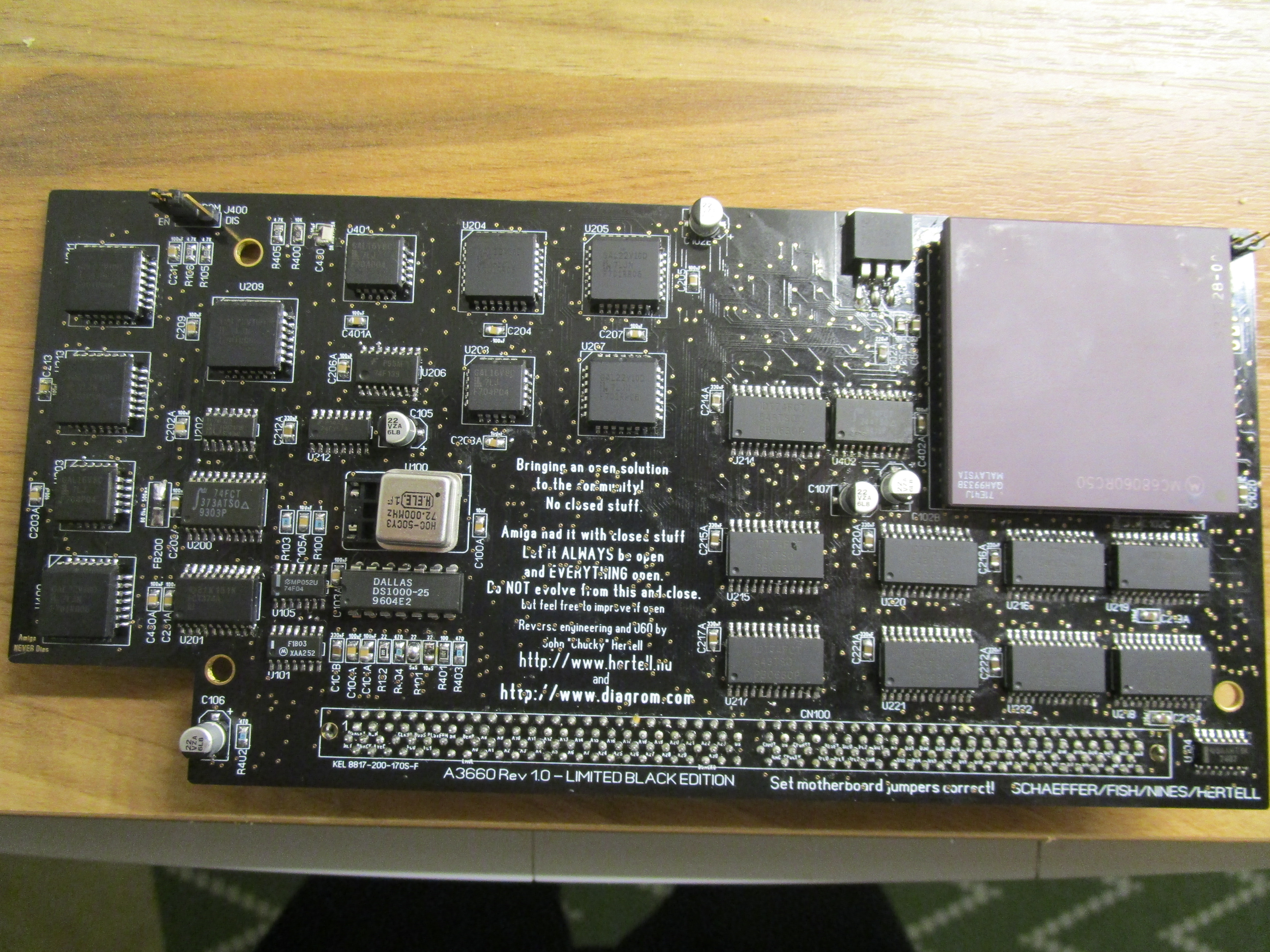
Well I did a first run of 20 board (I got 24) and I made them BLACK. My plan was to give those boards to people that have done good in the community. (AND I sold 2 in total)
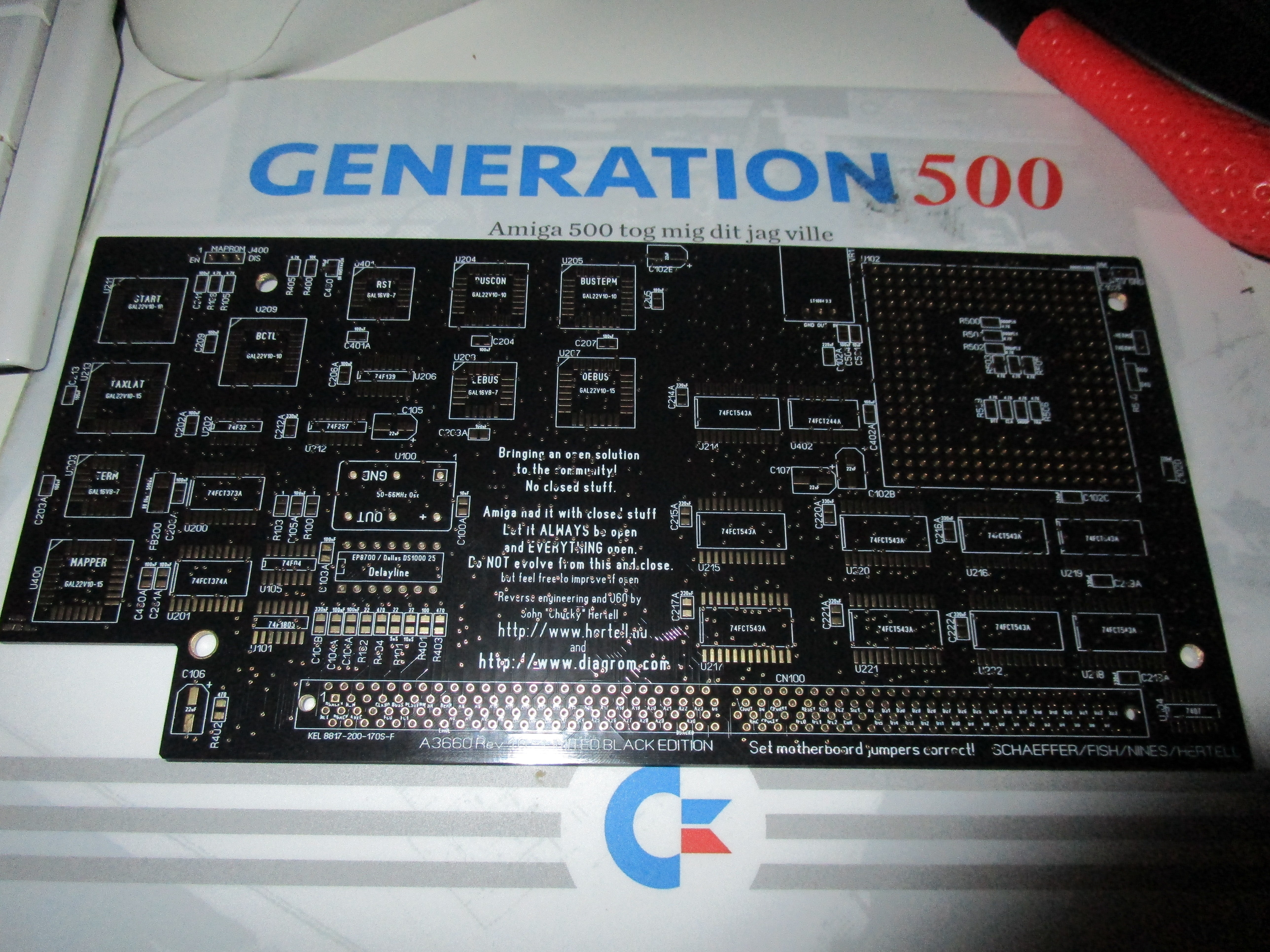
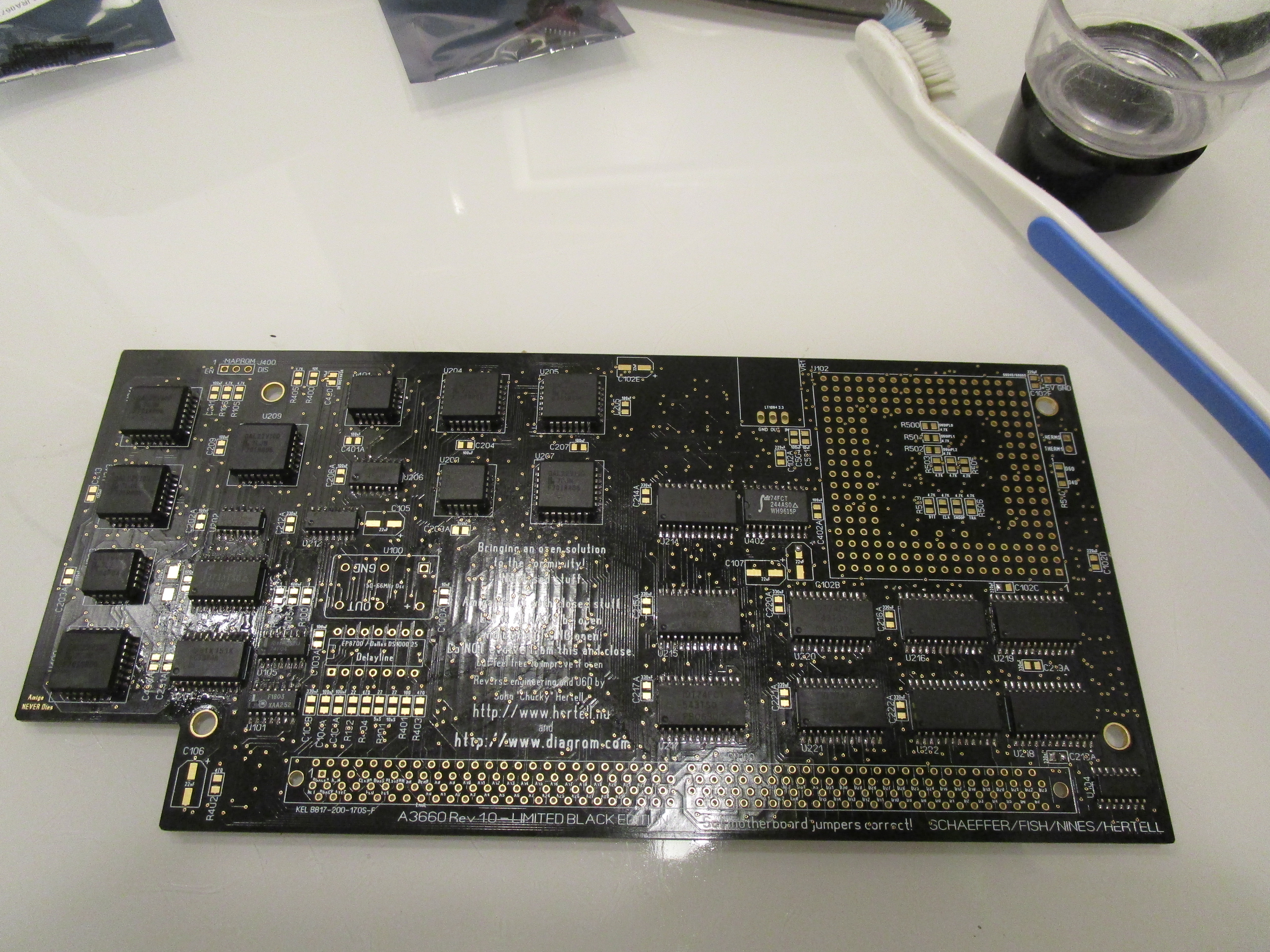
And this is the “final” build:
And if you look closly, there is a 72MHz osciallator installed. and IT SURE DID BOOT with it. but I would NEVER recomend you going higher than 66 as overclocking (over 50MHz) will overclock parts of the motherboard and might create issues.
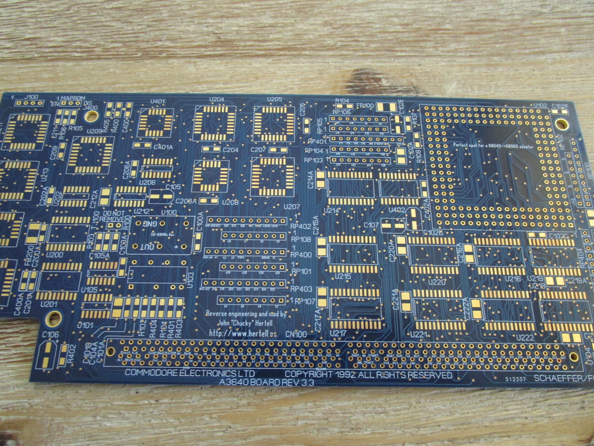
but at aprox 21:00 the 9:th of september this year, the A3660 booted for the first time. after some minor solderissues. (the resistors that replaces the resistorpacks are a TIGHT solder.. it is easy to short a via. I have actually changed that area in the files I will release here to make that more easy, but the boards I made after this have the same layout as the black board (but being blue).
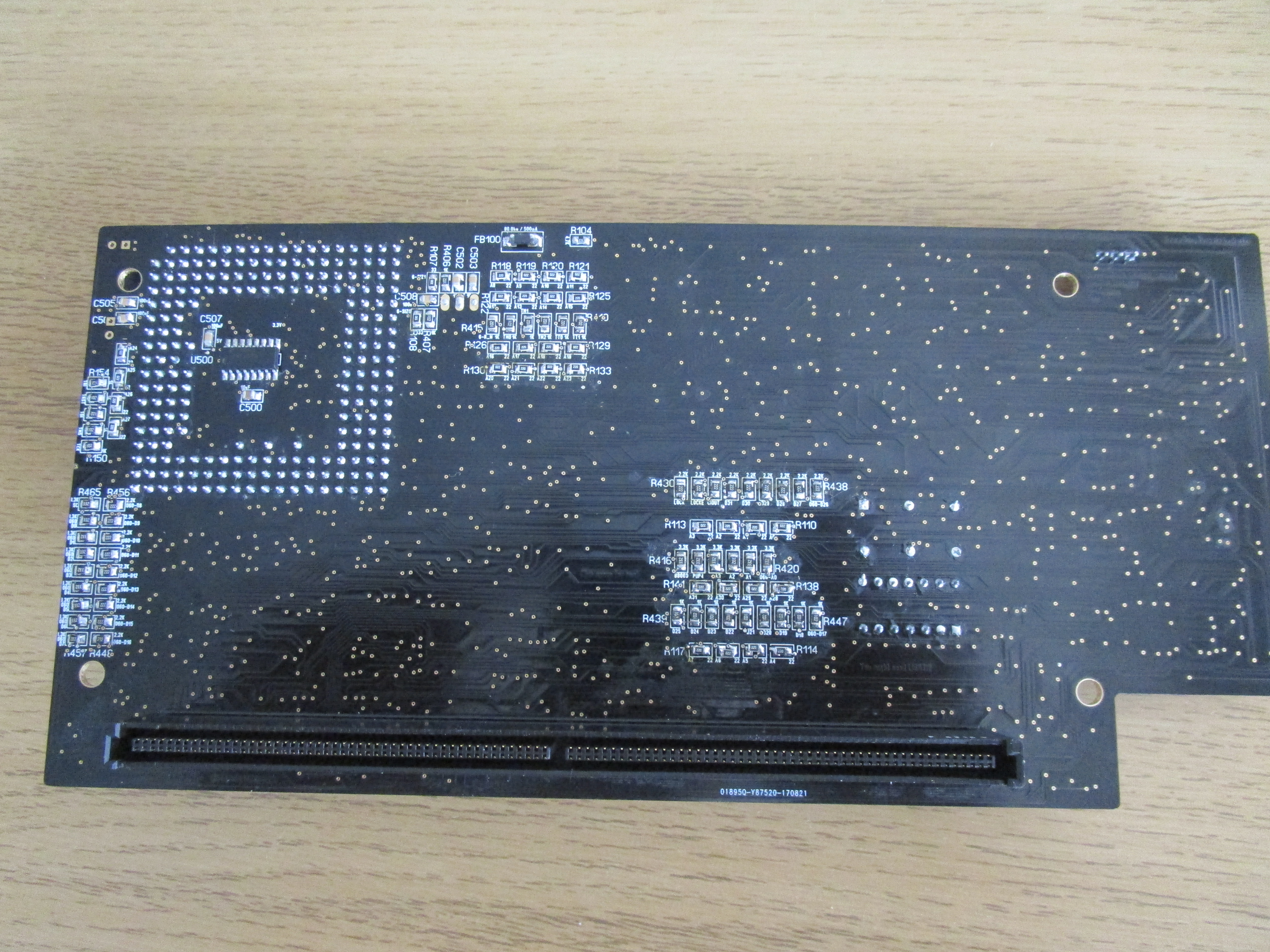
After doing that 3660 board I removed all gals, put in sockets and also inserted a 68060 compatible ZIF socket.. this is for me to use when I test GALs or CPUs. and this nice baby looks like this:
Front:

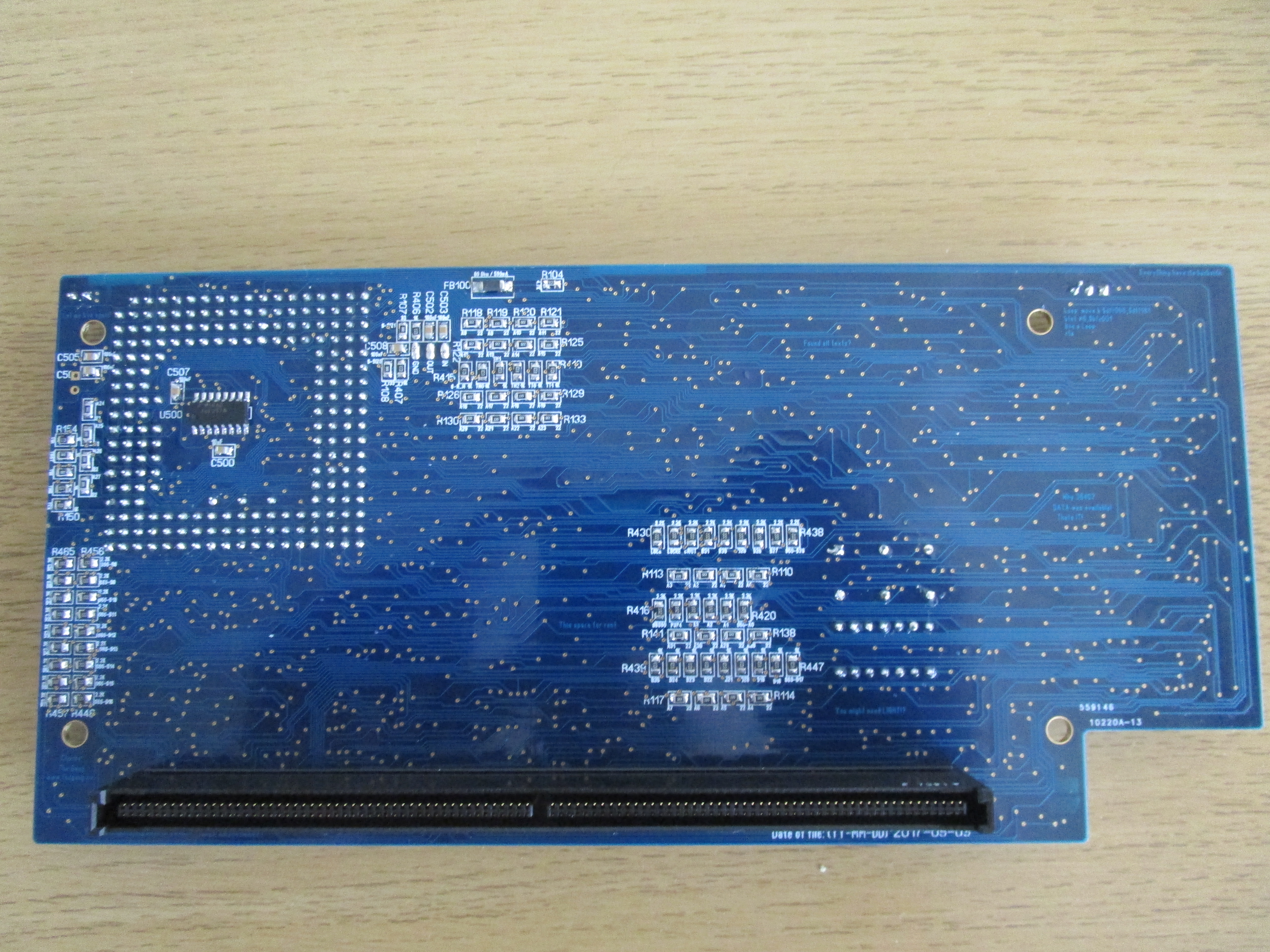
Back:
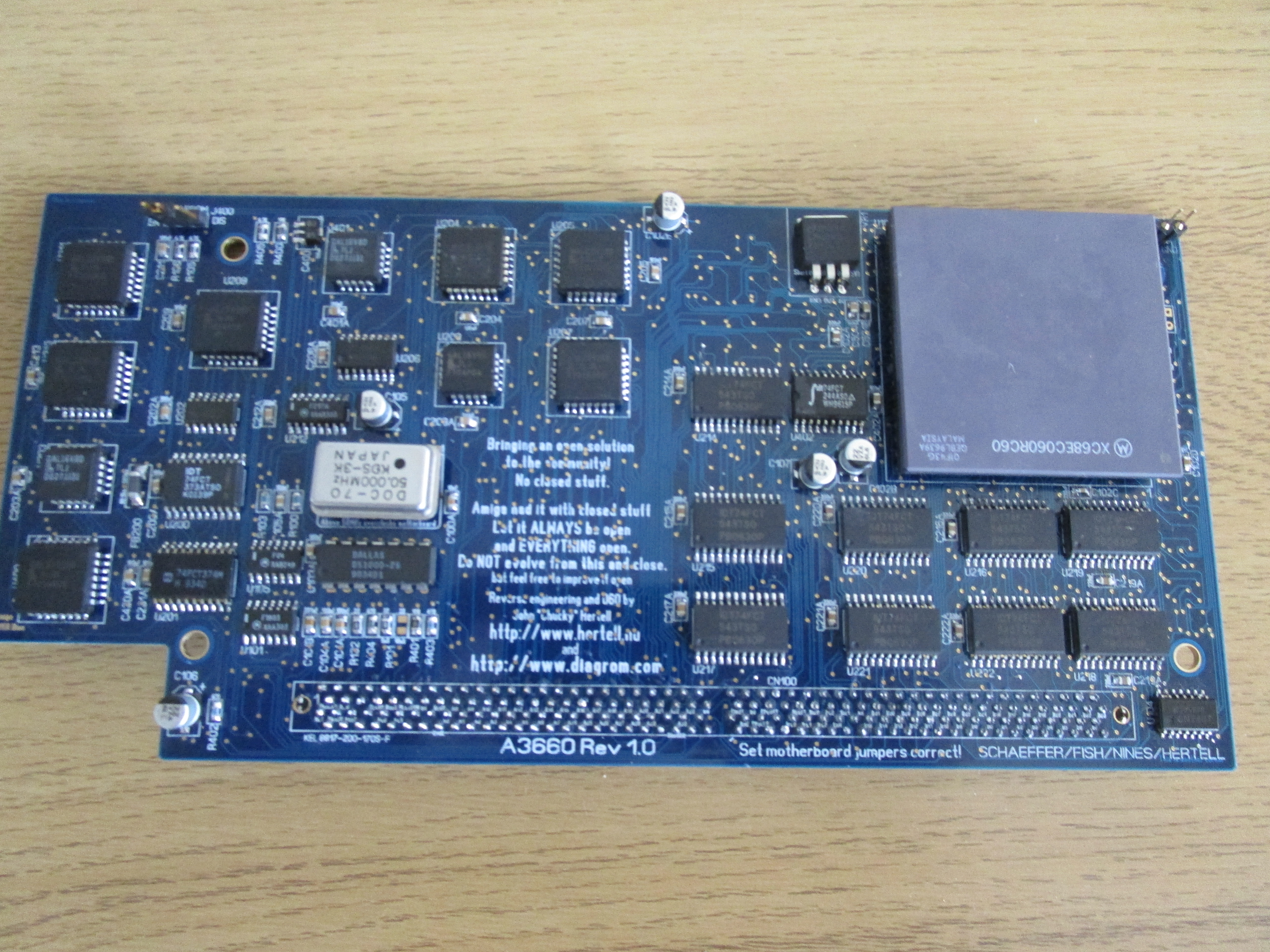
And a fully assembled BLUE board with no sockets etc: (This board you can have a look at on Amiga32 as I will bring it)
However.. lets talk about OPEN!.
YES! you will be able to download ALL my files. you are free to do own pcbs. you can sell them,. you can offer repairservices, I do not care what you charge, if you do it as a private person or company.. the important thing is that you offer the possability of getting people to use 040/060.
BUT! please, PLEASE , PLEASE to not use this data and do something own and close it.. THEN I will be pissed. and only then.
This solution is released (and shown) first at Amiga32 in Neuss. sure there is people knowing about this (especially those who already had got their black boards) but I have not spoken anything about this in forums.. actually just for the fun to show it as a surprise at Amiga32.
There is technically NO difference between the black or the blue boards. it is just that the black boards are for me to show some people that I like what they are doing for the community.
Also I will sell PCBs for 35Eur, this will contain some SMALL changes (like small eastereggs) compared to the boardfiles shown here. and the only reason for that is that you will get some support/help with solderissues if you bought those cards. I will try to help but cannot physically help you if you done the PCBs on your own. But there is NO technical differences between them.
WHAT is the next step? Well I will move this data to eagle so you can develope this. I am NO hardwaredesigner atall. but PLEASE talk with me if you have ideas. let us make this great. and lets not make double-jobs.
BUT THE FILES!?? I NEED THEM NOW!!!
Yup.. I bet.. ![]()
Here you can have all files to make PCBs for the A3640 Rev 3.3.2:
http://www.hertell.nu/webfiles/A3640Rev33.zip
And here all files for the A3660 Rev 1:
http://www.hertell.nu/webfiles/A3660Rev1.zip
I used seeedstudio to produce the boards using this:
PCB Dimension – 97.5mm*206.2mm
Surface Finish – ENIG
Min Solder Mask Dam – 0.4mm↑
Copper Weight – 1oz.
Half-cut / Castellated Holes – no
Min Hole Size – 0.3mm
PCB Color – Blue
Material – FR-4 TG130
Layer – 4 layers
Blind Vias – no
PCB Thickness – 1.6
Min Tracking / Spacing – 5/5 mil
GALs is still the A3640 ones:
So the original GAL files can be downloaded from: www.hertell.nu/webfiles/A3640.zip
There is also a hack to remove 2 waitstates improving memoryspeed. This CAN be instable if you use a quaddoubler.
But works fine with the 68060: Hack is made by speedgeek and can be downloade from:
www.hertell.nu/webfiles/A3640_ST_MOD.zip
(just replace the GALs in this archive from the A3640 ones. and you are ready to go)