Articles from Techtravels Amiga Blog
Primary tabs

Cirrus Logic CS4335 DAC problems finally identified and fixed.
I had some assistance in fixing this problem. My always helpful friend Brian from Canada as well as some help from Steve @ the Audacity forums contributed to solving the problem. They filled in some blanks for me, and encouraged me to LOOK at the data to see the problem.
This is the “Quit thinking and look” solution found in this book called “Debugging Rules”. Absolutely love this book!! Amazon link.
left-justified DAC problems continue
Here you see the analog sound waveform coming out of the DAC at the top in yellow.
I think I’m getting closer……I switched from the I2S DAC to a left-justified DAC just because the LJ one is a little simpler to design around….the MSB for the DATA is lined up with the LRCLK transition……
The digital channels below are the input to the DAC:
D3 is the serial data
D2 is SCLK
D1 is LRCLK
D0 is the MCLK
Trying to debug my design for an Audio DAC Cirrus Logic CS4334
I purchased a CS4334 to eventually use as an Audio DAC for the badge computer. I’ve never worked with DACs before, and my knowledge of audio is somewhat limited.
This audio DAC is a Cirrus Logic CS4334 with datasheet available here.
This chip is the I2S variant, specifically not the LEFT justified or RIGHT justified one. Each variant has slightly different timing requirements. The I2S specification is located here.
J68 is now booting from User Flash Memory on the BEMICRO MAX10 FPGA board
I’ve been struggling for quite a few nights and weekends over the last month or so.
I’ve now successfully attached the J68 to the built-in User Flash Memory. This means that the 16KB (actually about ~13KB) of the ROM monitor VUBUG is now out of the pre-initialized m9k’s configured as a ROM, and now into FLASH. Which is non-volatile, and will survive a reboot. The most important part of this is that it frees up our valuable high-speed on-chip m9k’s.
Still debugging the attachment of User Flash Memory to the J68….
So if I take my working UFM avalon-mm Master controller (which if you recall, connects to the Altera Flash Memory IP core), and attempt to attach it to the J68, the J68 no longer boots the ROM monitor code.
Since it’s not booting, I really don’t have many indications as to why. I decided that writing a ROM bus sniffer that records ROM memory requests and responses, including how long it took to satisfy that request, was worth the trouble.
In the image below, you’ll see four 32-bit columns of data on the left. Each row is a separate request.
They are:
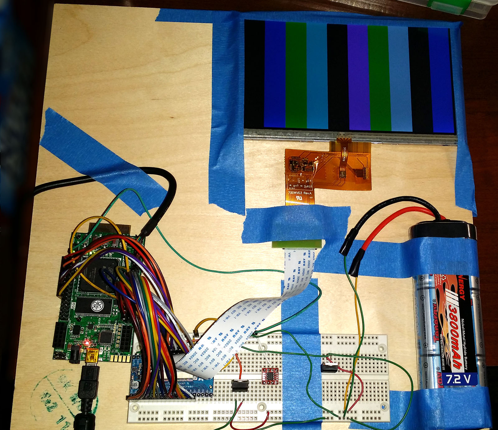
LCD Test image and pixel-level detail
So I’ve managed to get a semi-working test pattern image up on the LCD.
Here are a couple shots:
Reverse engineering the LCD interface
So I was having trouble getting the LCD working initially, so I ended up probing a working HDMI to LCD converter board sold by adafruit. You see, this board was driving my LCD just fine, but my FPGA couldn’t do diddly. So I wanted to see what I was missing.
This proved more difficult because of these 40-pin FPC connectors. Not sure what the pitch is, but it’s really freakin’ close together.
With a lighted magnifier (3x diopter?), and sharp o’scope probe, I was able to isolate individual pins on the 40-pin, long enough to hit the stop button on the scope.