Working on the User Flash Memory
So the Altera Max 10 FPGA we’re using has 256kbits of User Flash Memory. This is non-volatile memory that is built into the actual FPGA itself. This means you don’t need any external memory to get the FPGA to boot itself.
You can use the memory in several different combinations, depending on what you want to do. For instance, you can store a couple FPGA configurations (bitstreams that contain data to program the LUTs internally to “make” the hardware). I believe there’s a jumper on the eval board to allow you to select which one it should boot from. Pretty neat — like dual booting. (which is what they actually call it) In this case, using the flash that way is called CFM — configuration flash memory.
You can also use it as UFM, or User Flash Memory, where you store data for your particular application.
Right now, we are booting this badge computer with the J68 softcore with vubug.txt. (see main project page for the link, or google). This ROM Monitor, made in 1988(!!), is currently stored in the m9k’s (RAM blocks of the FPGA) but is taking up a precious 16K bytes of them. We really need these m9k’s for other things, like high-speed storage for other hardware peripherals, like the GPU.
One minor problem that I’ve discovered: the flash memory has pretty high latency. The m9k’s have none — the clock cycle after a read request, the right data is on the line. While never stated directly in any datasheet/manual that I could find, I saw some reference to a 5-cycle latency. I set off to measure this directly to make sure.
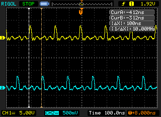
The top yellow line, CH1 on my Rigol 1102E, shows the READ request going out to the Avalon-MM (memory mapped) IP Core generated by Quartus II. Using the core is the only way to access the Flash memory.
The bottom line blue line, CH2, shows the Read Data Valid pin coming back from the memory.
As you can see with the measurement cursors, there’s 100ns delay between the request, and the data being on the line. At the current test speed of 50mhz(1/50mhz = 20ns), that’s five clock cycles. Exactly what I thought.
I am pre-initializing the UFM with a MIF file during programming. For this purpose, you need to make sure to program using the .POF file, and NOT the .SOF file, because the SOF doesn’t contain the data required for the programming of the flash. Programming flash takes longer than just writing the FPGA configuration, so that’s how you know it’s “working.”
I wrote a small state machine, along with my UART from a few projects back, that simply copies the contents of FLASH memory out of the serial port at 115.2K.
Here’s a screenshot
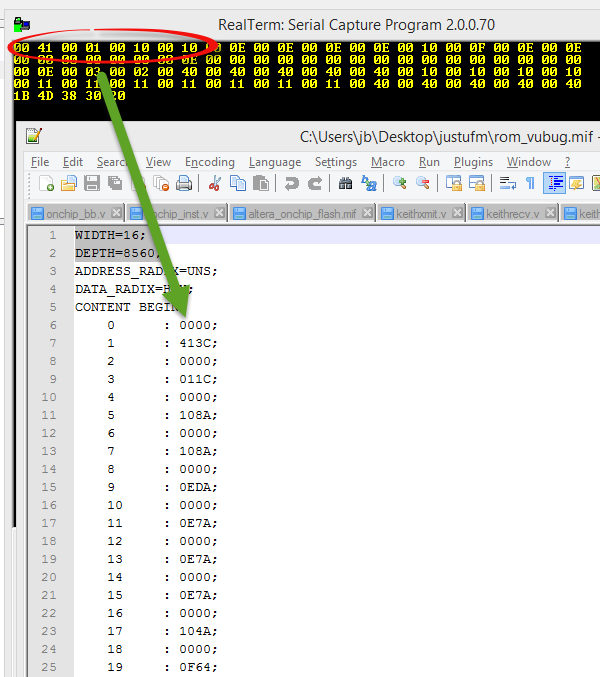
The key thing to note here is that only the high-order/MSB byte is being copied out of the port.
The next step for this effort is to attach the J68’s 16-bit wide bus, that is currently attached to the ROM via an m9k, and attach it to the UFM, which is 32-bits wide. There’s a super lossy way to do this, by simply ignoring the other 16-bits, but I hope I have time to do better than that!