Still debugging the attachment of User Flash Memory to the J68….
So if I take my working UFM avalon-mm Master controller (which if you recall, connects to the Altera Flash Memory IP core), and attempt to attach it to the J68, the J68 no longer boots the ROM monitor code.
Since it’s not booting, I really don’t have many indications as to why. I decided that writing a ROM bus sniffer that records ROM memory requests and responses, including how long it took to satisfy that request, was worth the trouble.
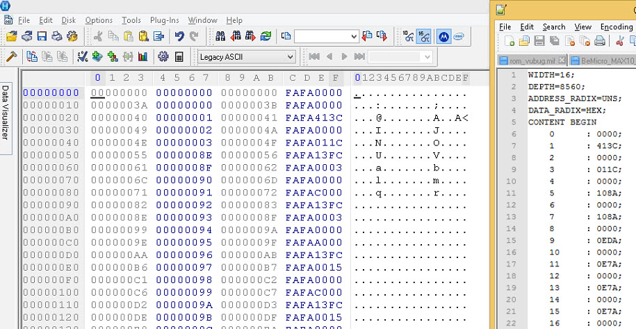
In the image below, you’ll see four 32-bit columns of data on the left. Each row is a separate request.
They are:
- A 32-bit counter that increments once a master clock cycle. Right now, I’m just running at 33.333mhz, but this J68 works upwards to 100mhz. This is recorded at the time of the request — at the time rd_ena goes high.
- The ROM memory address being requested (first column on the left in BLUE)
- The 32-bit counter at the time data_ack goes high, which means the request has been handled
- The actual 16-bit data value. Ignore the 0xFAFA — that’s just padding. (rightmost column in BLUE)
Note that the requests are being handled the next clock cycle, right now, with the M9k’s serving up the ROM file. So you see 0x3A request, 0x3B response. 0x40 request, 0x41 response, and so on. The flash will not be as quick, and there should be something like (5) cycles between them.
My plan is to attach my newly working debugger to the new J68 solution with the UFM, and compare it. I think the problem will be obvious once I see what is happening…..
