J68 can now speak with BEMICRO MAX 10 onboard SDRAM
So for the longest time, I’ve wanted to use the onboard 8MB SDRAM that is present on the BEMICRO MAX 10 fpga eval board. This is now a reality!
I’ve successfully integrated a controller with some glue logic to connect to the J68.
I’ve mapped the $20000-$81FFFE to the SDRAM. All calls to ROM (stored on-FPGA FLASH) are retrieved properly, some low level RAM calls access the on-FPGA M9K memory blocks, and the UARTs are all handled fairly seemlessly.
Here’s the very simple 68K memory check routine. Obviously this can be expanded on, but it’s passing!!
lea $20000,a6
chklop:
move.w a5,(a5)
andi.w #$0000,d5
move.w (a5),d5
cmp.w a5,d5
bne.w printfailz
suba.l #$000002,a5
cmpa.l a5,a6
bne.w chklop
lea passesz,a0
bsr writs
rts

Sometimes the results of success are with minimal fanfare. That’s ok with me. I understand how important this is to the project. With the J68 now being able to speak with the memory, there’s no limit in the number of applications.
There’s much more to do, though.
- There is so much room for optimization everywhere.
- The glue logic is probably very conservative. Working takes priority over speed.
- I’ve got the J68 CPU at 66.67mhz, but I’ve probably got room to take it to around 90mhz.
- The memory controller itself doesn’t allow for queued up reads.
- There’s no cache, which should really help things.
- I’ve got to add a simple priority arbiter for the wishbone interface to the memory. Other things have got to have access too. Like the video driver.
- I’m currently using the ROM monitor (see previous posts for link) VUBUG.TXT to boot. This is unnecessary but we barely know what we’re doing here. Eventually, I’d like to pare down the monitor, and get the UART setup code for the console port (only a few lines of assembly), and keep some of the utility routines. Booting mostly our own code is the goal.
- I’ve managed to add a new command the “f”-command for finally fu*king working to the rom monitor. It calls a batch of assembly, and that’s where my SDRAM test code from above sits. This gives us a way of calling our code and having access to some form of library routines.
- Right now, I’ve got to recompile the whole system, and reprogram the whole system. I should be able to rewrite just the MIF in on-fpga flash (UFM, as it’s called) which contains memory initialization code containing the 68K machine code which spit out from the assembler.
- and much more……..
I did manage to write a module (or two) that drives a small sainsmart serial LCD:

This allows me to display up to (8) 32-bit numbers in hex on the display at one time. Could be really useful in the future.
I also bought one of these Papilio Computing shield, because we need connectors! This is the cleanest presentation I’ve found, and should interface easy enough.
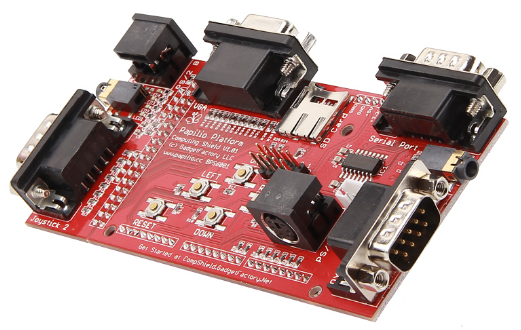
The most important interfaces are probably the VGA, for a monitor, and a couple of PS/2’s for keyboard and mice. The serial ports and audio could be real useful, too. Certainly the SDCARD slot.
So the project is moving along nicely!