Introducing the Re-Amiga 1200
tl;dr: Files at bottom of this post ![]()
One slow day (12th of june 2018) being on a hotel doing work for one week I asked on facebook on the “Commodore Amiga” group:
”Reversetime. What pcb do you think I should reverse? Come with ideas. A board often damaged by battery or caps. Preferbly smaller ones. So give me hints of.. “whats next”
I got several ideas. CV64, CD32 etc. then I got the. ”Amiga 1200 I have a empty PCB”
So. I asked for a scan of that PCB and got it So that’s why I decided, YES! I will do this. I have a lot of dead 1200s at home and leakage killed alot.
So.. he (Folkert De Gans) scanned it for me. and I started to work on it. this is the reason why it is the Rev 1D.4 and not the latest. that is what we had.
AND. it is also by far the most common board anyway.
I started Sprint Layout and started to do my work.
This is the scanned pictures of the PCB:
BUT! for the mother of god. WHY SPRINT!?
This is a very good and legit question. to design stuff in Sprint is a total nightmare. BUT if you want to make a copy of a PCB. it is fast, really fast and you DO get a gerber in the end. this is why. I totally know that for development it is utter crap. but it lets me get my job done. We can do more PCBs I am happy. I might try to figure out a way to move this data to eagle/kicad or whatever. but until then. I will do more stuff in sprint.
if you want to have a look at the workfile, the demoversion works very well downloadable at:
https://www.electronic-software-shop.com/lng/en/electronic-software/sprint-layout-60.html
Anyway, back to topic
So it started with putting all components at the correct locations (kinda aproximate, not 100% exact position some 10th of millimeters off but good enough.
well.. in sprint you can have the scanned picture as a background:
and then just simply “draw” traces above the scanned picture. and this is why it works so fine for a job like this.
While talking about this on Facebook, another person (Nico Blüthmann) told that he could send me a dead a1200 pcb to help me. and he did.
I decided to remove all components and sand it down to the copper, so silkscreen etc doesn’t confuse me.
So I did:
Now drawing traces is just a matter of time:
Here you can see how I have drawn traces above the scanned picture. Anyway. now it is just the very timeconsuming time to draw everything. and also checking the scans many many MANY times over. did I miss a trace to a via. did I…. I also used http://www.amigapcb.org/ alot by selecting pins of every chip see where it did go. measure on my boards and use the test function in sprint if everything was connected.
and when all traces was done, I “just” had to find what vias should be connected to GND or VCC. and then.. I was done!
BUT. I wanted to do stuff. so what did I want to do?
first of all, the CXA chip for composite is EOL, it also requires some hard to get delaylines (the square weird components close to the powerconnector)
and a friend of mine is doing this nice S-Video/Composite/RGB Adapter: http://electronics.chroma.se/svideo.php
So why not put THAT stuff there instead, RF modulator will be removed. I asked him and got his eagle-workfiles and permission to use his design.
so I did.
I also made traces to power/gnd to the CPU thicker, I made generally all powertraces thicker.
I also added connectors for keyboard like the rev2 PCB of the A1200, and IRQ7 possability, and a jumper so IF you want to mess with the floppy SEL signals you can do this without any strange socketsolutions.
did this. and ordered a testrun of the PCB:

And I started to solder it. it DID start.. but.. my DiagROM only showed flashing backgroundcolors, but nothing on screen.
I checked my files against scanned picture and all . everything LOOKS ok. until I suddenly come to think of one thing. Commodore have this throughhole resistor mounted on the pads between ALICE and the FPU Place. and after playing with it. YES.. it now worked.
I also had an issue with I had a stuck FIRE1 pressed on joyport 1 all the time. this was as when I soldered I had some missing components so I moved from the old pcb. it showed that one ceramic cap was shorted doing this. lesson learned: NEVER move passives from the old PCB.
some other minor issues all depending on having the wrong value of components etc at some locations. I HAVE sold some pre-release PCBs. IF you have please click on this link to download an errratafile how to fix this. Updated 2018-08-17: http://www.hertell.nu/webfiles/R1200-Issues.docx
Anyway. I got all working. AND it also does boot a BPPC 60MHz 68060, 330MHz PPC with 128MB ram from a stock light 4.5A Amiga PSU, something my original 1D.4 PCB doesnt do.
so the ReAmiga 1200 is an Amiga 1200 Rev 1D.4 with the following changes:
- Supports Round AND Square powerconnector. (round have 2 incoming +5V wires)
- New reworked Composite logic, with additional S-Video Support
- RF-Modulator removed and replaced with optional VGA Connector that is buffered, Still NO Scnadoubler
- Selectable SEL signals for floppy, you need to cut the traces and solder in a connector to select:
- Optional NMI (IRQ7) Possability
- Resetheader
- A500 Compatible Keyboard connector (actually not tested yet)
- Support for the Ratteswitch with solderoles for required signals so no need of a socket on CIA.
- Extra powerconnectors for +12 and +5V fans. also extra powerconnector close to CPU slot to add power or fans.
- PCMCIA Reset fix so cardreset software is not needed.
- Optional onboard leds where LED and +5V are separated also optional “opt” led, with jumperwire for pcmcia activityled.
I have tested this board for several hours, with Apollo 1260, Blizzard PPC, Blizzard 1230 MK2, MBX 1230. no issues.
BUT this IS a hobby project, I leave no warranty etc.
So BUILDING the shit? well I will do a post later about this when I get the “production” pcbs showed here in this post. as this post would be too long anyway.
Are you screaming for the FILES?
Well sure. as I want stuff to be open I try to open most of my work. this is no exception:
first of all the Amiga 1200 clone. THIS IS NOT TESTED WHATSOEVER. You are on your own! but if you do a pcb and it works and send to me, first person doing that I will send an ReAmiga PCB as exchange:
http://www.hertell.nu/webfiles/A1200-CLONE.zip
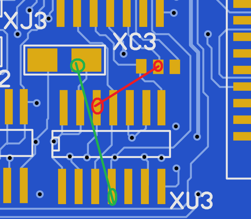
Remember the patch I missed:
SOME solutions need a wire between the 2 red marked places. this is for the budgie.
and some needs a 47Ohm resistor between the 2 green slots. or you will not get any picture.
Well Enough of the old 1200. Lets check the ReAmiga files:
http://www.hertell.nu/webfiles/ReAmiga1200.zip
- Analysis Results
- layers : 4
- minimum trace width : 5,9 mil
- minimum trace spacing : 5,14 mil
- minimum drill size : 0,3 mm
- width : 354,9 mm
- height : 182,18 mm
So basically 5/5 Mil tolarance and 0,3mm drillings
for the R1200 there is a BOM file as txt and excel, for the clone you are on your alone.
If you need help where to solder the different components you can use the tool my friend TSB did:
http://www.hertell.nu/locator/locator.php?project=r1200
A tool I will use for all my future projects.
Where to get chipsets? well no idea! My reason to do this is to make old dead machines live again. my experience is that most faults on 1200s isn’t the chipset but corroded PCBs and shorted ceramic caps etc. so put in all new passives. move the chipset and logic and connectors and VOILA!
And here is a youtube link of me testing this some hours ago: https://www.youtube.com/watch?v=PlxLs2KYNKw
You CAN buy PCBs from me, contact me for information. atleast the 2 first batches I will give 5 euro per sold PCB to the Swedish children cancer fond:
https://www.barncancerfonden.se/