Understand the system
Of all of the different techniques this one may be the simplest but also the most important.
When you’re trying to reverse engineer something, understanding the system is key to unraveling the black box which is the PAL. You need to understand what connects to the PAL on the inputs, what it connects to on the output side. Usually going one level back isn’t enough. Why? Because maybe the PAL connects to an OR gate, that then takes a couple other connections. So what you need to do is follow from the primary driver to the consumer of that signal.
You’ll need to collect as much documentation as you can about the system:
- Schematics
- Block diagrams
- User manuals
- generic google results like forum posts
- datasheets for each of the ICs
- Example application reference diagrams
The question you are trying to answer is a high-level one:
What is the main function of this PAL? What’s it’s purpose?
I started to create a bill of materials for the PCB in question, which essentially becomes a list of parts. This gives you a checklist to start collecting datasheets to read and improve my understanding. You’ll want three categories of parts for a BOM. Here’s an example list I created for my first PAL I re’d.
DataFlyer Plus Bill of Materials
Passives
- (3) resistors 180 ohm 5% 1/4W. Top left.
- (1) 104 E5M capacitor. Ceramic capacitor 100nf. Top left.
- (1) 045 RTK capacitor. Not sure about this one! Top right.
- (1) 47uf Electrolytic capacitor. Top right.
- (1) 220uf electrolytic capacitor. Bottom left.
- (1) resistor pack labeled 103. 10k ohm. 6 pins. https://www.digikey.com/en/products/detail/cts-resistor-products/77061103P/1000571
- (1) resistor pack labeled 102. 1k ohm. 6 pins. https://www.digikey.com/en/products/detail/cts-resistor-products/77061102P/1000573
- (1) 30 ohm resistor. Bottom right.
- (3) resistor pack labeled G on the board. https://www.digikey.com/en/products/detail/bourns-inc/4608X-104-221-331L/1089163
Headers
- (2) right-angle dual row male headers. One 26-pin header and one 50-pin header.
- (1) straight 86-pin dual row male header.
- (3) 2-pin male headers.
- (1) 3-pin male header.
Integrated circuits
- SN74F32N, which is a quad 2-input OR gate
- SN74LS244/245N (labeled 244/245 on silk screen)
- 74LS373, an octal latch
- 74F521N, an 8-bit comparator
- 27C256-15 ROM
- TIBPAL16L8-25CM labeled BUSS
- TIBPAL16L8-25CM labeled DTACK
- AM5380PC, the AMD SCSI controller chip
To understand the purpose of single part, it’s helpful to look to see what’s surrounding it.
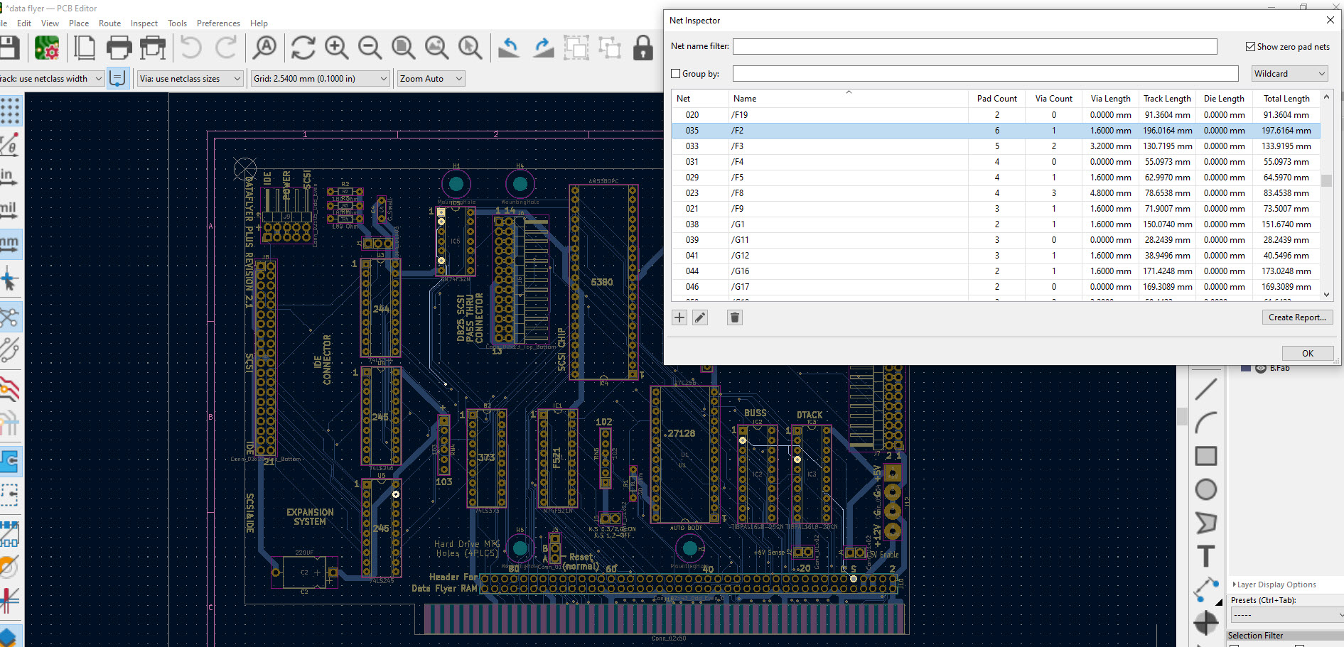
I didn’t have access to a schematic and so I started the tedious and error-prone “beeping out” using a multimeter for continuity. This soon got old and complicated, so I decided to unsolder all of those components on the top of the PCB, and take high-resolution photographs of the PCB. Then, I employed someone at Fiverr to create a Kicad schematic and gerbers for me. This gives me a nice interactive tool to figure out what’s connected to what.

So as you can see below, now I can easily trace different pins on the PAL (labeled BUSS on the PCB) and to where they connect.
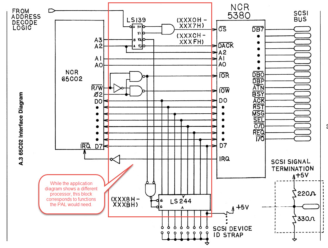
This image below from the 5380 datasheet shows the application diagram. Often time system designers copy directly from the reference application because it’s a tested, known, good implementation using the chip. It’s very possible the system designer looked at exactly this same diagram when building the card originally!
As you can see, getting as much information in front you, reading it, and understanding it is really key to being able to reverse engineer it.